Computer Systems Lab 2 - Logic Design
- Work environment
- Basic one – switch and light
- Inverter
- OR
- AND
- XOR
- Complex logic circuits
This lab aims to implement simple logic circuits. The software used is Log.ly The focus is to learn how to design the circuits, find the truth table for the gates, and simulate the combination of gates.
Work Environment
When you start Logic Friday, a blank canvas screen is provided for defining circuits.

There is a menu for handling project-specific tasks such as creating new diagrams and file management. To create a new logic gate diagram select File, New, and the Gate Diagram.
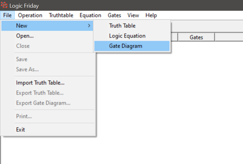
This will open the logic gate components window at the bottom-right of the main window.
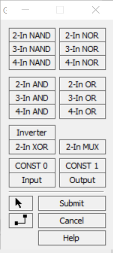
The components we can create are:
- NAND, NOR, AND, and OR gates. The 2-In, 3-In, and 4-In prefix defines the number of inputs the gates will take.
- An Inverter which is the NOT gate.
- A 2-In XOR gate.
- Constant 0 or 1 values.
- Inputs and outputs.
- Wires (the button next to Cancel).
Finding a Truth Table
We will now examine the truth table for an AND gate.
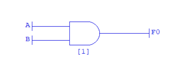
- Add a 2-in AND gate to the canvas.
- Add an Input to the canvas to the left of the AND gate. For the Variable Name leave it as default (A).
- Add a second Input to the canvas below the other Input. For the Variable Name leave it as default (B).
- Connect the two Inputs to the AND gate using a wire.
- Add an Output to the canvas to the right of the AND gate. For the Variable Name leave it as default (F0).
- Connect the AND gate to the Output using a wire.
Your diagram should look something like this:
Now, click the Submit button on the Components Window. The logic diagram will be analysed and the equation and truth table generated. Your screen will look something like this:
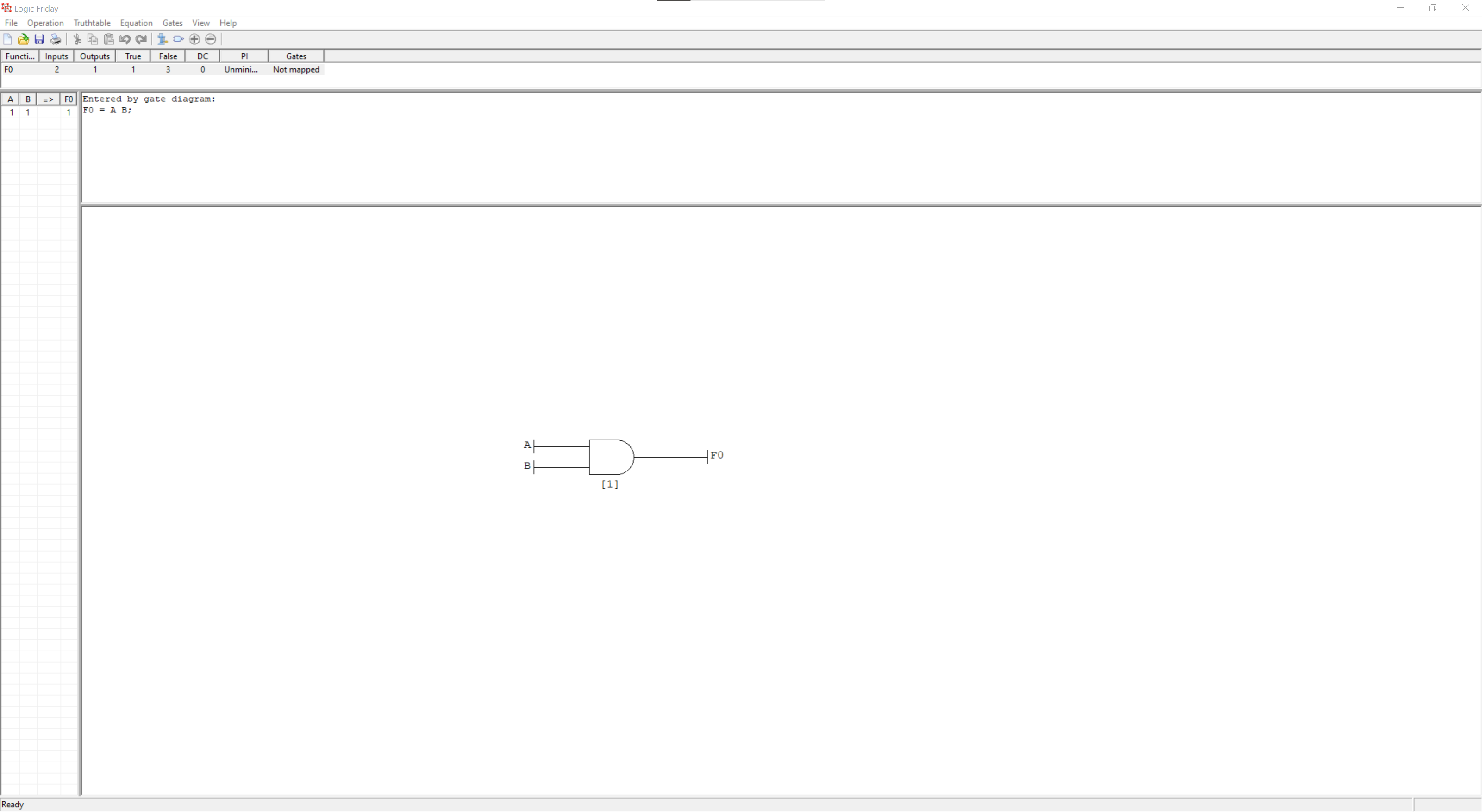
At the moment, only the 1 (true) outputs are shown on the truth table on the left. In the menu, select Truthtable then Show all rows. The full truth table will be shown.
Above the canvas, the function equation is shown. This is:
F0 = A B;
An AND gate is sometimes represented by multiplication (e.g., A B) rather than with the logical and symbol. An OR gate is sometimes represented by a plus (e.g., A + B) rather than with the logical or symbol. This does not matter for this lesson. We are only concerned with gates and truth tables.
Increasing the Inputs
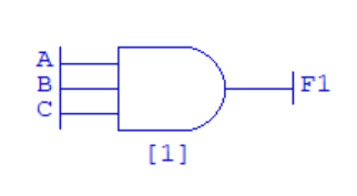
We can edit the gate diagram by clicking Gates then Modify Gate Diagram. Now perform the following steps:
- Delete the existing 2-In AND gate.
- Add a 3-In AND gate.
- Wire up the existing two Inputs and Output to the gate.
- Add a third Input (C) to the diagram and wire it to the gate.
- Click Submit to analyse the system.
- Select Truthtable then Show all rows to see all the rows.
Your diagram should be:
Exercises
- Find the truth table for OR, NOT, and NOR with two inputs.
- Find the truth table for a NAND with four inputs.
- Find the truth table for an XOR with four inputs (hint - you need three gates in total).
Working with Multiple Gates
Let us draw the logic circuit for the following:
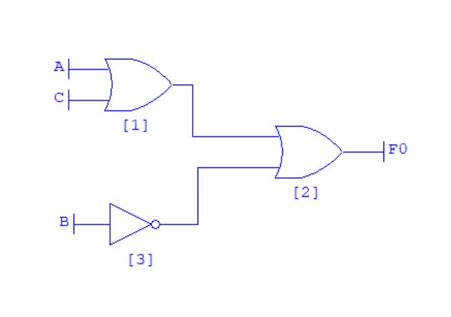
\[f = A \lor C \lor ¬B\]We will need two 2-in OR gates and one NOT gate (Invertor).
- Create a new Gate Diagram.
- Draw the three gates.
- Add three Inputs: A, B and C.
- Wire A and C into a single OR gate.
- Wire the output from this gate into the second OR gate.
- Wire B into the NOT gate.
- Wire the output from the NOT gate into the second OR gate.
- Add an Output F0.
- Wire the output from the second OR gate into F0.
Your diagram should look something like this:
Click Submit, then Truthtable, Show all rows to analyse the diagram. It should be the same as:
| A | B | C | => | F0 |
|---|---|---|---|---|
| 0 | 0 | 0 | 1 | |
| 0 | 0 | 1 | 1 | |
| 0 | 1 | 0 | 0 | |
| 0 | 1 | 1 | 1 | |
| 1 | 0 | 0 | 1 | |
| 1 | 0 | 1 | 1 | |
| 1 | 1 | 0 | 1 | |
| 1 | 1 | 1 | 1 |
Exercises
Implement the following logical expressions and derive their truth tables.
- \[¬(A \land B) \lor ¬B\]
- \[(A \land B) \lor ¬(B \land C)\]
- \[(A \oplus C) \land ¬B\]
- \[(A \land B \land (C \lor D)) \lor (C \land D)\]